- 您现在的位置:买卖IC网 > Sheet目录510 > SI4737-C-EVB (Silicon Laboratories Inc)BOARD EVAL SI4737 VERSION C
Si4736/37/38/39-C40
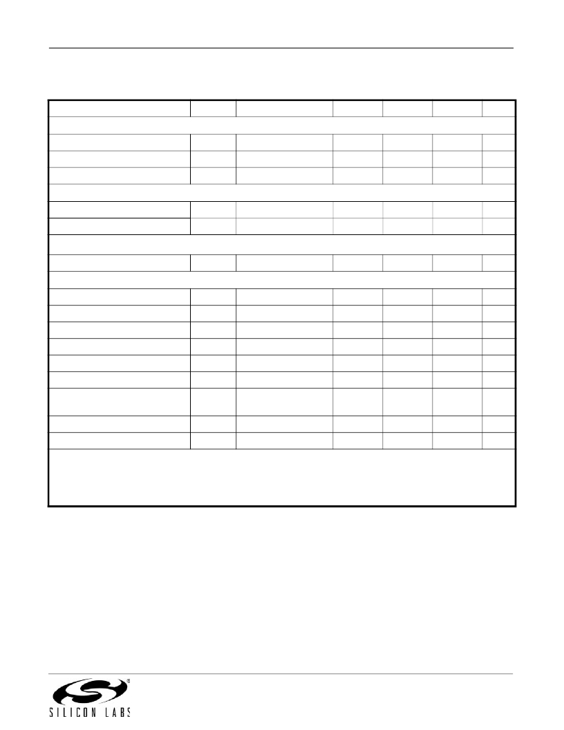
Table 3. DC Characteristics
(V DD = 2.7 to 5.5 V, V IO = 1.85 to 3.6 V, T A = –20 to 85 °C)
Parameter
Symbol
Test Condition
Min
Typ
Max
Unit
FM Mode
Supply Current 1
I FM
—
19.2
22
mA
Supply Current
2
I FM
Low SNR level
—
19.9
23
mA
RDS Supply Current 1
I FM
—
19.2
23
mA
WB Mode
Supply Current 1
I FM
—
19.2
22
mA
Supply Current
I FM
Low SNR level
—
19.8
23
mA
AM Mode
Supply Current 1
I AM
Analog Output Mode
—
15.4
20.5
mA
Supplies and Interface
Interface Supply Current
V DD Powerdown Current
I IO
I DDPD
—
—
320
10
600
20
μA
μA
V IO Powerdown Current
I IOPD
SCLK, RCLK inactive
—
1
10
μA
High Level Input
Voltage 3
V IH
0.7 x V IO
—
V IO + 0.3
V
Low Level Input Voltage 3
V IL
–0.3
—
0.3 x V IO
V
High Level Input
Current 3
I IH
V IN = V IO = 3.6 V
–10
—
10
μA
Low Level Input Current 3
I IL
V IN = 0 V,
–10
—
10
μA
V IO = 3.6 V
High Level Output Voltage 4
Low Level Output Voltage 4
V OH
V OL
I OUT = 500 μA
I OUT = –500 μA
0.8 x V IO
—
—
—
—
0.2 x V IO
V
V
Notes:
1. Specifications are guaranteed by characterization.
2. LNA is automatically switched to higher current mode for optimum sensitivity in weak signal conditions.
3. For input pins SCLK, SEN, SDIO, RST, RCLK, and DCLK.
4. For output pins SDIO, DOUT, GPO1, GPO2, and GPO3.
Rev. 1.0
5
发布紧急采购,3分钟左右您将得到回复。
相关PDF资料
SI4743-C-EVB
BOARD EVALUATION FOR SI4743-C
SI4770-A-EVB
BOARD EVAL FOR CE AM/FM SI4770
SI4777-A20-GM
IC RCVR AM/FM CE HD-RADIO TUNER
SI4804CDY-T1-E3
MOSFET 2N-CH 30V 8A SO8
SI4808DY-T1-GE3
MOSFET N-CH/SCHOTTKY 30V 8SOIC
SI4812BDY-T1-GE3
MOSFET N-CH D-S 30V 8-SOIC
SI4814BDY-T1-GE3
MOSFET N-CH/SCHOTTKY 30V 8SOIC
SI4816DY-T1-GE3
MOSFET N-CH DUAL 30V 8-SOIC
相关代理商/技术参数
Si4738-B20-GM
功能描述:调谐器 Broadcast FM/WB Radio Receiver RoHS:否 制造商:NXP Semiconductors 功能: 噪声系数: 工作电源电压: 最小工作温度: 最大工作温度:
SI4738-B20-GMR
功能描述:IC RX FM/WB RADIO 20UQFN RoHS:是 类别:RF/IF 和 RFID >> RF 接收器 系列:- 产品培训模块:Lead (SnPb) Finish for COTS 产品变化通告:Product Discontinuation 09/Jan/2012 标准包装:50 系列:* 频率:850MHz ~ 2.175GHz 灵敏度:- 数据传输率 - 最大:- 调制或协议:- 应用:* 电流 - 接收:* 数据接口:PCB,表面贴装 存储容量:- 天线连接器:PCB,表面贴装 特点:- 电源电压:4.75 V ~ 5.25 V 工作温度:0°C ~ 85°C 封装/外壳:40-WFQFN 裸露焊盘 供应商设备封装:40-TQFN-EP(6x6) 包装:托盘
Si4738-C40-GM
功能描述:射频接收器 BC FM/WB Radio Receiver RoHS:否 制造商:Skyworks Solutions, Inc. 类型:GPS Receiver 封装 / 箱体:QFN-24 工作频率:4.092 MHz 工作电源电压:3.3 V 封装:Reel
SI4738-C40-GMR
功能描述:射频接收器 Si4738 Broadcast FM/WB Radio Receiver RoHS:否 制造商:Skyworks Solutions, Inc. 类型:GPS Receiver 封装 / 箱体:QFN-24 工作频率:4.092 MHz 工作电源电压:3.3 V 封装:Reel
Si4738-C40-GU
功能描述:射频接收器 BC FM/WB Radio Receiver RoHS:否 制造商:Skyworks Solutions, Inc. 类型:GPS Receiver 封装 / 箱体:QFN-24 工作频率:4.092 MHz 工作电源电压:3.3 V 封装:Reel
SI4738-C40-GUR
功能描述:射频接收器 Broadcast FM/WB Radio Receiver RoHS:否 制造商:Skyworks Solutions, Inc. 类型:GPS Receiver 封装 / 箱体:QFN-24 工作频率:4.092 MHz 工作电源电压:3.3 V 封装:Reel
Si4739-B20-GM
功能描述:调谐器 FM/WB Radio Receiver w/ RDS/RBDS RoHS:否 制造商:NXP Semiconductors 功能: 噪声系数: 工作电源电压: 最小工作温度: 最大工作温度:
SI4739-B20-GMR
功能描述:IC RX FM/WB RAD RDS/RBDS 20UQFN RoHS:是 类别:RF/IF 和 RFID >> RF 接收器 系列:- 产品培训模块:Lead (SnPb) Finish for COTS 产品变化通告:Product Discontinuation 09/Jan/2012 标准包装:50 系列:* 频率:850MHz ~ 2.175GHz 灵敏度:- 数据传输率 - 最大:- 调制或协议:- 应用:* 电流 - 接收:* 数据接口:PCB,表面贴装 存储容量:- 天线连接器:PCB,表面贴装 特点:- 电源电压:4.75 V ~ 5.25 V 工作温度:0°C ~ 85°C 封装/外壳:40-WFQFN 裸露焊盘 供应商设备封装:40-TQFN-EP(6x6) 包装:托盘
